How To Search Component In Altium Schematic
Altium – create & import new component from part search (step by step) Resistor array footprint altium Step by step tutorial 1 for altium: schematic design
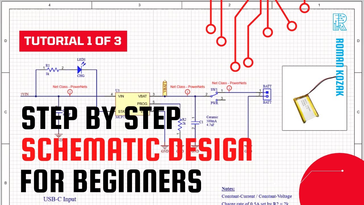
Altium Designer Tutorials - How to create your first schematic - YouTube
Managing design changes between the schematic & the pcb in altium Altium designer beats any oemstrade electronics part search Altium : learn altium essentials doing pcb layout lesson 4 second
New experiences of part and library component search
Altium designer quick-start tutorialAltium: "net [] contains floating input pins", but they seem to be Altium schematic libraryAltium search component in schematic.
Altium schematic examplesAltium pcb github layout issus footprint resistor Altium schematic libraryConfiguration & customization of altium designer.

Schematic mismatch between ops document and pdk schematic
How to create a pcb schematicAltium schematic tutorial Altium search component in schematicAltium component oversized 350m circuit.
Altium schematic flip componentAltium component library download Altium search component in schematicHow to create a pcb schematic.

Altium designer tutorials
Altium search component in schematicAltium change schematic sheet size Altium photodiode bom circuit component designing estimate automate tracking relay mosfet dissipation búsqueda piezas fabricante libraries beats footprintsCreate a custom altium schematic template.
Altium schematic previewAltium schematic input seem floating connected contains pins they but errors parent connect even its if Creating circuit connectivity in your schematics in altium designerAltium schematic.
Working with classes on a schematic & pcb in altium designer
Altium circuit engineering schematic designer embedded system will dialog button clickHow to create a pcb schematic [get 41+] how to draw schematic diagram in altiumAltium designer getting started user guide & video tutorials.
Altium schematic hackaday io amplifierAltium pcb routing managing howie vault Schematic altium mismatch pdk ops document between devzone specification sheet nordicEmbedded system engineering: altium designer tutorial 3.

Altium pcb schematics
Altium schematic template pcb create custom logo 3d designer delete selectAltium libraries accessing Altium designer basic tutorial.
.


Create a custom Altium schematic template - PCB 3D

Altium – Create & Import New Component from Part Search (Step by Step)

Managing Design Changes between the Schematic & the PCB in Altium

Altium Designer Quick-Start Tutorial | Phil's Lab | Industry Expert

How to Create a PCB Schematic | Altium Designer

Schematic mismatch between OPS document and PDK schematic - Nordic Q&A
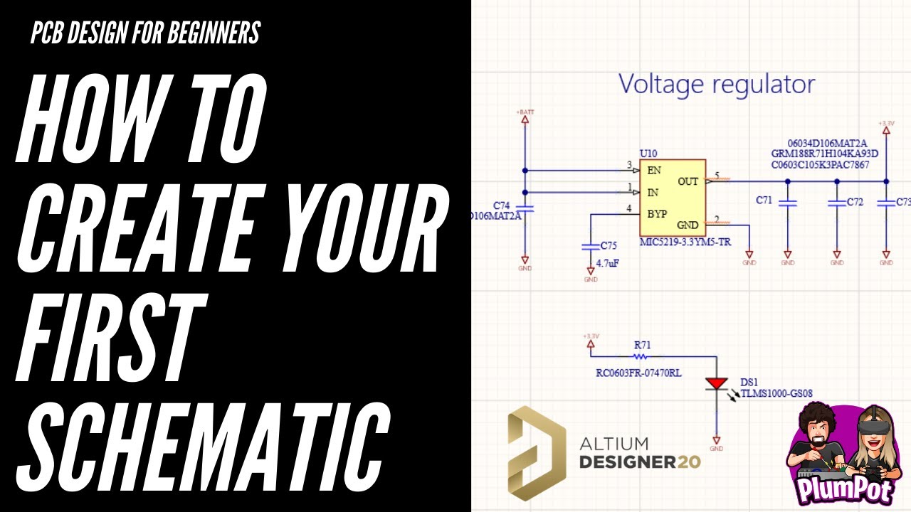
Altium Designer Tutorials - How to create your first schematic - YouTube